
Imec and EV Group have demonstrated wafer-to-wafer hybrid bonding at a 200-nanometer copper interconnect pad pitch. The result, presented this week at ECTC 2026, was achieved on a test vehicle with routable interconnects and is aimed at future logic-to-logic and memory-to-logic stacking. The Leuven research hub says it reached a copper pad-to-pad post-bond overlay vector below 40 nanometers for all dies across a full 300-millimeter wafer. For context, Imec last year reported wafer-to-wafer hybrid bonding at 300nm pitch with overlay error less than 25nm for 95 percent of the dies and feasibility to further extend the roadmap to a 250nm pitch.
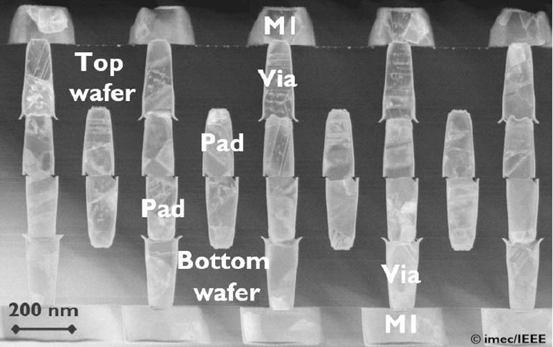
Making the interconnect pitch smaller increases the number of vertical connections that can fit between stacked chips, increasing the bandwidth and lowering the latency. As the pitch scales, so do the requirements for the bonding overlay between two Cu pads. In general, the required overlay accuracy of the bonding process corresponds to one-fourth of the pitch.
“This breakthrough fine-pitch hybrid bonding result was achieved by co-optimizing all the critical elements of Imec’s hybrid-bonding process flow. These include, among others, the use of SiCN as the dielectric material and a chemical mechanical polishing step prior to bonding. The latter was optimized for high across-wafer uniformity to produce extremely flat dielectric surfaces while achieving a controlled few nanometers of recess for the Cu pads. The high overlay accuracy and control, enabled by EVG’s wafer bonding tool, were additionally facilitated by an improved Cu pad design and by pre-bond lithography corrections,” comments Zsolt Tokei, Imec fellow and program director of 3D system integration.