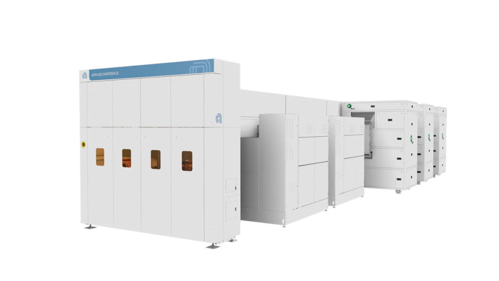
Applied Materials and Besi launched a fully integrated die-to-wafer hybrid bonding platform at Semicon West. Bits&Chips attended the press meeting about this system called Kinex during Semicon Europe in Munich.
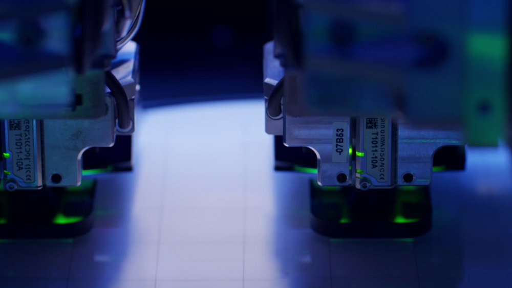
With the introduction of the Kinex system by Applied Materials and Besi, their strategy for scaling hybrid bonding (HB) into high-volume logic and memory production has become more visible. Kinex is a fully integrated system. The process from wafer preparation to chiplet management and bonding is executed in a closed environment.
This closed environment actually contains everything that needs attention in a semiconductor context. In addition to precision and – still poor – throughput, this includes cleanliness. Because the material preparation, chiplet management and placement process in the Kinex is completely sealed off from the outside world, the system is also suitable for future use in assembly factories such as OSATs that don’t achieve the cleanliness levels of front-end fabs.